

SUMMARY DESCRIPTION
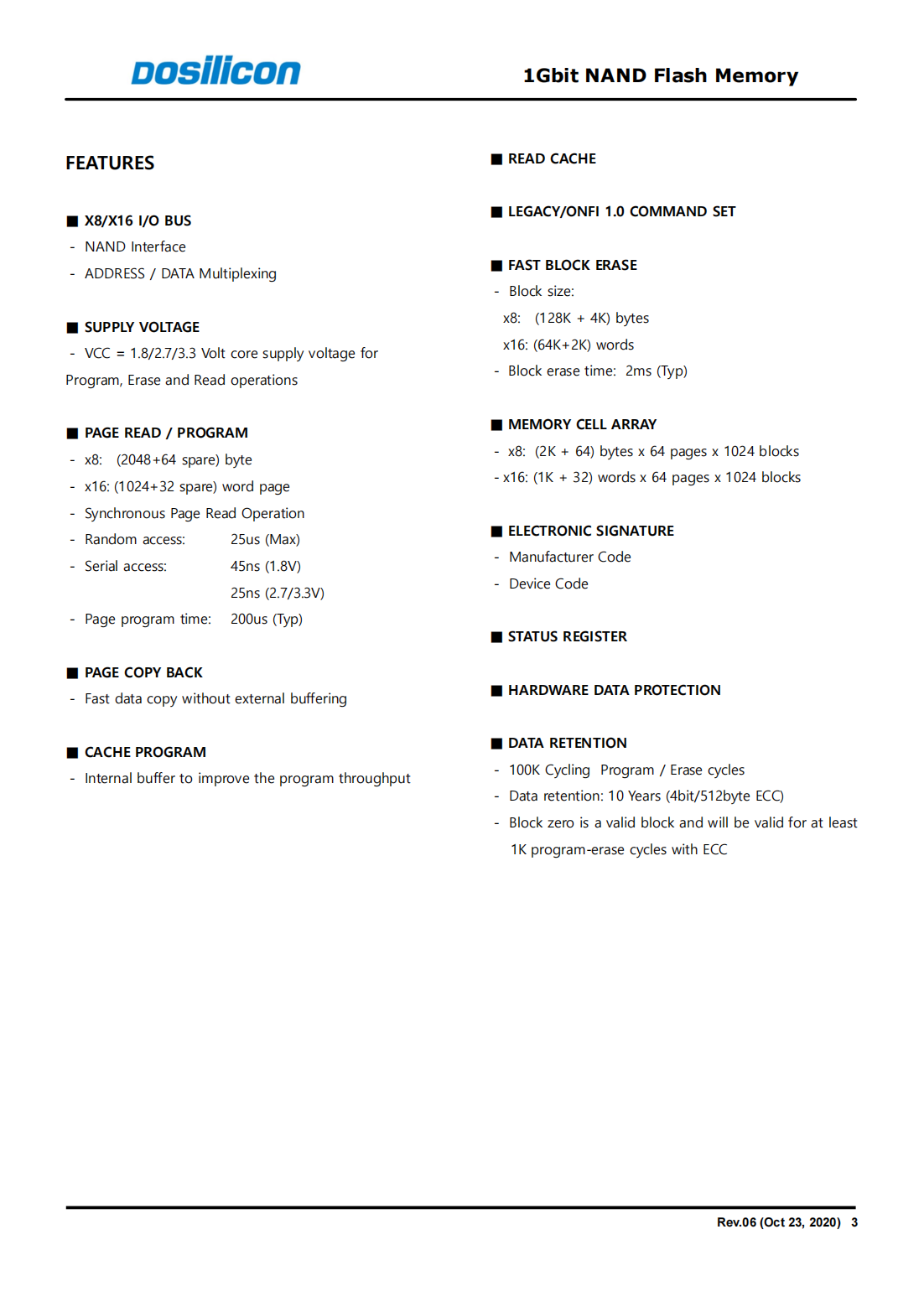
FMND1GXXXXX is a 128Mx8bit with spare 4Mx8(x8),64Mx16bit with spare 2Mx16(x16)bit capacity.The device is offered in 3.3/1.8 Vcc Power Supply,and with x8 and x16 I/O interface.The memory is divided into blocks that can be erased independently so it is possible to preserve valid data while old data is erased.
The device contains 1024 blocks,composed by 64 pages consisting in two NAND structures of 32 series connected Flash cells.Program operation allows the 2112-byte page writing in typical 200us and an erase operation can be performed in typical 2 ms on a 128K-byte block.Data in the page can be read out at 25ns cycle time per word(2.7/3.3V version),and at 45ns cycle time per word(1.8V version).The I/O pins serve as the ports for address and data input/output as well as command input.This interface allows a reduced pin count and easy migration towards different densities,without any rearrangement of footprint.Commands,Data and Addresses are synchronously introduced using CE#,WE#,ALE and CLE input pin.
The on-chip Program/Erase Controller automates all program and erase functions including pulse repetition,where required,and internal verification and margining of data.The modify operations can be locked using the WP#input pin.
This device supports ONFI 1.0 specification.
The output pin RB#(open drain buffer)signals the status of the device during each operation.In a system with multiple memories the RB#pins can be connected all together to provide a global status signal.


 18677706250
 咨詢
咨詢